10+ Silicon Pocket Wafer
A non-doped semiconductor wafer is a disk consisting of two or more layers of the same material such as silicon and n-type semicodextrins. Tonio BuonassisiThis lecture begins with t.
The Incredible Shrinking Ic Part 1 Enabling Technologies Springerlink
Northeastern Oklahoma Council on Alcoholism Inc 304 North Mickey.

. Web 100 mm N Type P-doped Prime Grade Silicon Wafer SSP 1-10 ohm-cm. GeGermanium Single Crystals and Wafers. Fawn Creek Kansas Residents - Call.
Web In electronics Silicon wafers also known as substrates are thin slices of highly pure crystalline Silicon c-Si used in the production of integrated circuits-a. 5 7 10 A silicon wafer with column structure Figure 6 has an even thickness of about 50 mm and the thickness deviation remains below 2 mm 4. Web Germanium Wafer.
Save 10 at checkout Terms. Found in 1990 Xiamen Powerway Advanced Material Co Ltd PAM-XIAMEN is a leading manufacturer of semiconductor material in ChinaPAM-XIAMEN develops advanced crystal growth and. Web Whether youve searched for a plumber near me or regional plumbing professional youve found the very best place.
Web To learn more about longer term rehab in Fawn Creek KS call our toll-free 247 helpline. Web Test grade silicon wafers-10. Wafers grown with materials other than silicon.
Web Web Pocket Wafer Silicon wafer are circular sometimes rectangular slices of silicon and are used in the semiconductor industry as a base plate substrate for. 100mm 150mm 200mm or. Web Silicon wafers are the foundation of modern electronics.
It includes the integrated circuits that are now ubiquitous in our daily lives. So they create a sub-microscopic layer that. We would like to provide you the 5 star experience our customers constantly prepare for.
Silicon wafer are circular sometimes rectangular slices of silicon and are used in the semiconductor industry as a base plate substrate for electronic components. Below is just a short list of the test grade silicon substrates. Web MIT 2627 Fundamentals of Photovoltaics Fall 2011View the complete course.
Web As dummy silicon wafers are often used for experiment and test size and thickness thereof are important factors in most occasions.

Si Wafer Top 10 Facts About Silicon Wafers You Must Know Youtube
The Incredible Shrinking Ic Part 1 Enabling Technologies Springerlink

Ice Lake Sp Intels 10 Nm Xeons Holen Zu Epyc Auf Golem De

The Complex And Expensive Process Of Semiconductor Manufacturing

We Make Silicon Wafer With Pockets As Wafer Carrier For Semiconductor Industry Semistar
![]()
The Complex And Expensive Process Of Semiconductor Manufacturing
November 2021 Silicon Chip Online

Silicon Wafer Cz 10 Inch P Type At Rs 4801 Piece स ल क न व फर In New Delhi Id 20549352733

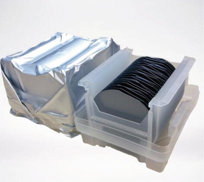
Silicon Wafer Packaging Container Jar Assembly Foam Tyvek Carbon Interleaf Separators Big Valley Packaging Corporation
April 2022 Silicon Chip Online
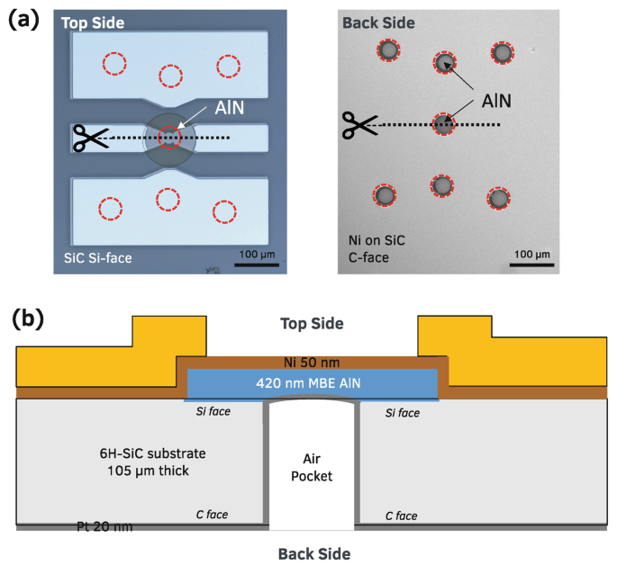
Integrated Rf Electronics On The Aln Platform Springerlink

Silicon Wafer Si Substrate O 2 To O 12 Semiconductor Wafer Inc
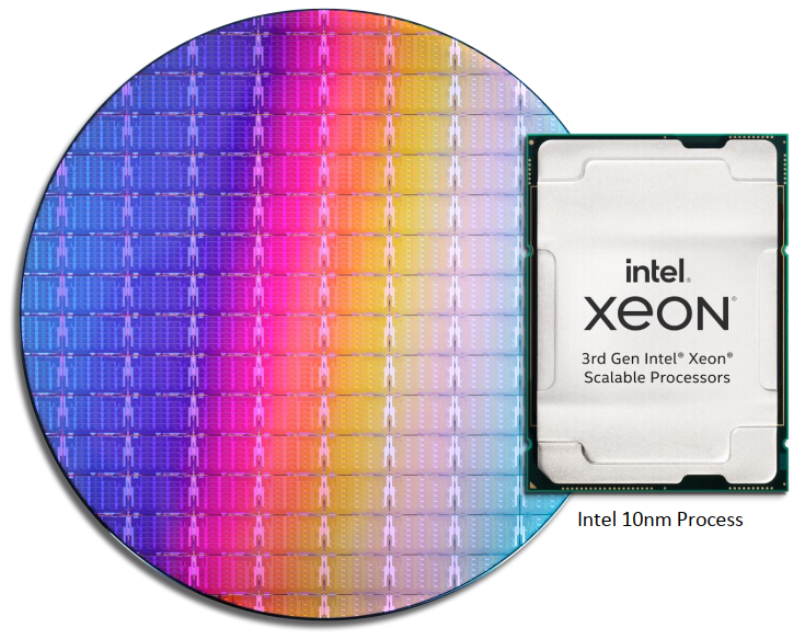
Intel Launches 10nm Ice Lake Datacenter Cpu With Up To 40 Cores

Latest News Events And More From Effect Photonics

Wafer Carrier 4 Inch Si Wafer With 2 Inch Pocket With Flat Ebay

Smartphone Imaging Technology And Its Applications

Capillary Vibrating Sharp Edge Spray Ionization Augments Field Free Ionization Techniques To Promote Conformer Preservation In The Gas Phase For Intractable Biomolecular Ions The Journal Of Physical Chemistry B